|
Plasmonic Laser Nanoablation for lithography |
 |
|
Current Research
|
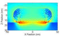
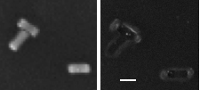
Top: Computational electric field enhancement for infrared laser light incident on a gold nanorod on a silicon surface. Bottom: SEM images of nanorod ablation. Scale bar: 50 nm.
|
Moore’s Law, first stated in 1965, was an observation that computer chip density doubled every two years and that it should continue to do so for the foreseeable future. This prediction has proven remarkably prescient over the last 40 years. However, conventional lithography is limited to half of the wavelength used in fabricating features for micro? and nano?electronic devices and current fabrication technology is approaching the size limits given available light sources. Increasingly sophisticated methods are now being used to develop smaller features, but increasing cost and complexity and the existence of a fundamental limit render these methods unsustainable. In light of this problem, fabrication methods that can create features smaller than the diffraction limit are of great interest. One possible nanofabrication method is the use of plasmonic laser nanoablation. Our research focuses on the use of plasmonic laser nanoablation for fabricating nanostructures. We use computational techniques to investigate the interaction between laser light and gold nanoparticles while experimentally creating nanoablation features on silicon and glass substrates using plasmon?enhanced femtosecond laser pulses.
|
|